Write in front
PCB production is very complex. Taking a four-layer printed board as an example, the production process mainly includes PCB layout, core board Production, inner PCB layout transfer, core board punching and inspection, lamination, drilling, copper chemical precipitation on the hole wall, outer PCB layout transfer and outer PCB etching and other steps. Today we will learn about the production process through animations.
Source: EUROCIRCUITS, mechanical master
PCB production process
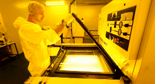
01
PCB layout
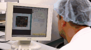
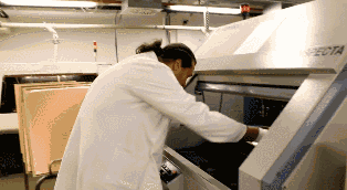
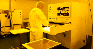
No. 1 in PCB production The first step is to organize and check the PCB layout (Layout). The PCB production factory receives the CAD files from the PCB design company. Since each CAD software has its own unique file format, the PCB factory will convert it into a unified format - Extended Gerber RS-274X or Gerber X2. Then the factory engineers will check whether the PCB layout complies with the manufacturing process and whether there are any defects or other problems.
02
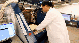
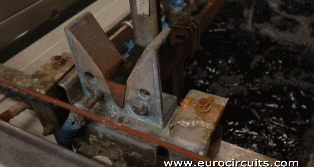
Production of core board
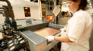
Clean the copper clad laminate, If there is dust, it may cause the final circuit to be short-circuited or broken.
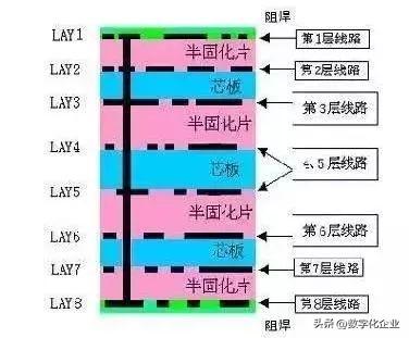
The picture below is a The illustration of an 8-layer PCB is actually composed of 3 copper-clad laminates (core boards) plus 2 copper films, which are then glued together with prepreg. The production sequence is to start from the middle core board (4th and 5th layer circuits), continuously stack them together, and then fix them. The production of 4-layer PCB is similar, except that only one core board and two copper films are used.
03
Inner PCB layout transfer
First make the most The two-layer circuit of the intermediate core board (Core). After the copper clad laminate is cleaned, a layer of photosensitive film will be covered on the surface. This film will solidify when exposed to light, forming a protective film on the copper foil of the copper-clad laminate.
Connect the two layers of PCB Lay out the film and double-layer copper-clad laminate, and finally insert the upper PCB layout film to ensure the accurate stacking position of the upper and lower PCB layout films.
UV for photosensitive machines The light irradiates the photosensitive film on the copper foil. Under the light-transmitting film, the photosensitive film is cured, but under the opaque film, there is still no cured photosensitive film. The copper foil covered under the cured photosensitive film is the required PCB layout circuit, which is equivalent to the role of laser printer ink for manual PCB.
Then use lye Clean the uncured photosensitive film, and the required copper foil circuits will be covered by the cured photosensitive film.
Then use strong Alkali, such as NaOH, will etch away unwanted copper foil.
Place the cured photosensitizer Tear off the film to expose the required PCB layout circuit copper foil.
04
Core board drilling and inspection
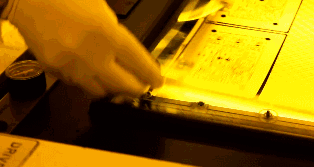
The core board has been produced success. Then punch alignment holes on the core board to facilitate alignment with other raw materials.
Once the core board is PCBs on other layers cannot be modified if they are pressed together, so inspection is very important. The machine will automatically compare it with the PCB layout drawing to check for errors.
05
Laminating
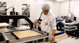
Need a new one here The raw material is called prepreg, which is the adhesive between the core board and the core board (PCB layer number > 4), as well as the core board and the outer copper foil, and also plays an insulating role.
The lower copper foil The two layers of prepreg have been fixed in position through the alignment holes and the lower iron plate in advance, and then the prepared core board is also placed in the alignment holes. Finally, the two layers of prepreg, a layer of copper foil and a layer of pressure-bearing sheet are placed in sequence. The aluminum plate covers the core plate.
will be ironed The clamped PCB boards are placed on the bracket and then sent to the vacuum heat press for lamination. The high temperature in the vacuum hot press can melt the epoxy resin in the prepreg and fix the core boards and copper foils together under pressure.
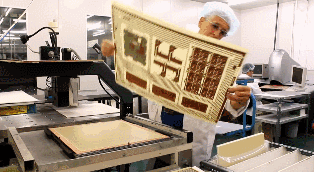
After lamination is completed , remove the upper iron plate that suppresses the PCB. Then take away the pressure-bearing aluminum plate. The aluminum plate also plays the role of isolating different PCBs and ensuring that the outer copper foil of the PCB is smooth. At this time, both sides of the PCB taken out will be covered by a layer of smooth copper foil.
06
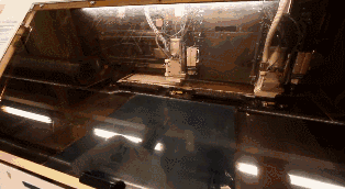
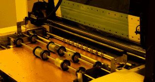
Drilling
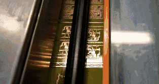
Four layers of copper foil that are not in contact are connected together. First, holes through the top and bottom must be drilled to open up the PCB, and then the hole walls are metallized to conduct electricity.
Drill with X-Ray The hole machine positions the inner core board. The machine will automatically find and locate the holes on the core board, and then punch positioning holes on the PCB to ensure that the subsequent drilling passes through the center of the hole.
Place a layer of aluminum plate Place on the punch machine and place the PCB on top. In order to improve efficiency, 1 to 3 identical PCB boards will be stacked together for perforation according to the number of PCB layers. Finally, cover the top PCB with an aluminum plate. The upper and lower layers of aluminum plate are to prevent the copper foil on the PCB from tearing when the drill bit drills in and out.
On the previous layer During the pressing process, the melted epoxy resin was squeezed out of the PCB, so it needed to be removed. The master milling machine cuts the periphery of the PCB according to its correct XY coordinates.
07
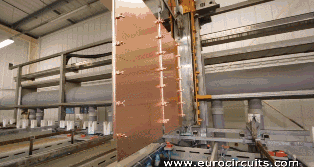
Chemical precipitation of copper on the hole wall
Since almost all PCB The designs all use perforations to connect circuits on different layers. A good connection requires a 25 micron copper film on the hole wall. This thickness of copper film requires electroplating, but the hole walls are composed of non-conductive epoxy and fiberglass sheets.
So the first step It is to first deposit a layer of conductive material on the hole wall, and then form a 1 micron copper film on the entire PCB surface, including the hole wall, through chemical deposition. The entire process such as chemical treatment and cleaning is controlled by machines.
Fixed PCB
Cleaning PCB
Shipping PCB
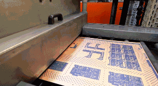
08
Outer PCB layout transfer
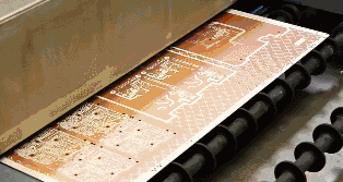
Next The outer PCB layout is transferred to the copper foil. The process is similar to the previous inner core board PCB layout transfer principle. Both use photocopied film and photosensitive film to transfer the PCB layout to the copper foil. The only difference is that it will be used Positive film making board.
Inner PCB layout The transfer adopts the subtractive method, using negative film as the plate. The circuits covered by the cured photosensitive film on the PCB are cleaned and the uncured photosensitive film is removed. After the exposed copper foil is etched, the PCB layout circuits are protected by the cured photosensitive film and remain.
Outer PCB layout The transfer is done using the normal method, using the positive film as the board. The non-circuit area covered by the cured photosensitive film on the PCB. Clean the uncured photosensitive film and proceed with electroplating. Areas with a film cannot be electroplated, but areas without a film must be plated with copper first and then tin. After the film is removed, alkaline etching is performed, and finally the tin is removed. The circuit pattern remains on the board because it is protected by tin.
Clip the PCB Clamp and plate the copper. As mentioned before, in order to ensure that the hole position has sufficient conductivity, the electroplated copper film on the hole wall must be 25 microns thick, so the entire system will be automatically controlled by a computer to ensure its accuracy.
9
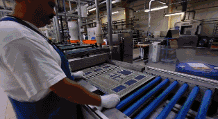
Outer PCB etching
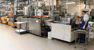
Next is a A complete automated assembly line completes the etching process. First, clean off the cured photosensitive film on the PCB board. Then use strong alkali to clean off the unnecessary copper foil covered by it. Then use tin stripping liquid to remove the tin plating on the copper foil of the PCB structure. After cleaning, the 4-layer PCB layout is completed.
Articles are uploaded by users and are for non-commercial browsing only. Posted by: Lomu, please indicate the source: https://www.daogebangong.com/en/articles/detail/PCB-dian-lu-ban-zhi-zuo-gong-yi-guo-cheng-zhan-shi-dong-tai-tu-jie.html
 支付宝扫一扫
评论列表(196条)
测试